Push Pull Amplifier Schematic Diagram. The advantage of push pull amplifier is that there is no power dissipated in output. Working of push pull transistor circuit.
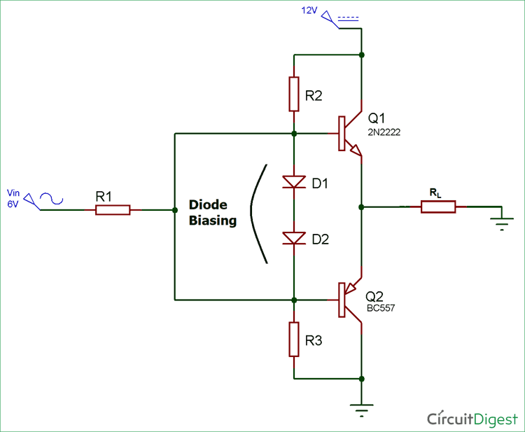
These two transistors can be of type bjt or mosfet. The push pull amplifier is designed based on the above circuit diagram. But unlike class a in class ab biasing resistor values are selected such that the transistors q1 and q2 are biased just above the cut in voltages.
In our analysis of the circuit we will consider the class b amplifier.
In the circuit diagram two transistors t1 t2 are placed back to back. When the input signal is positive q1 starts conducting and produce a replica of the positive input at the output. Circuit diagram of class ab push pull amplifier. But unlike class a in class ab biasing resistor values are selected such that the transistors q1 and q2 are biased just above the cut in voltages.
