Common Collector Amplifier Diagram. In electronics a common collector amplifier also known as an emitter follower is one of three basic single stage bipolar junction transistor bjt amplifier topologies typically used as a voltage buffer. The input is to be applied at the base terminal.
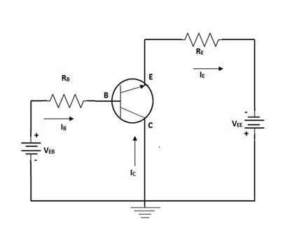
Although the common collector amplifier is not very good at being a voltage amplifier because as we have seen its small signal voltage gain is approximately equal to one a v 1 it does however make a very good voltage buffer circuit due to its high input z in and low output z out impedances providing isolation between an input signal source from a. Common collector amplifier has collector common to both input and output. Called the common collector configuration its schematic diagram is shown in figure below.
The collector is to be treated common for both input and the output sides or sometimes considered to be grounded.
In this circuit the base terminal of the transistor serves as the input the emitter is the output and the collector is common to both for example it may be tied to ground reference or. The collector is to be treated common for both input and the output sides or sometimes considered to be grounded. The common collector amplifier our next transistor configuration to study is a bit simpler for gain calculations. The input is to be applied at the base terminal.
