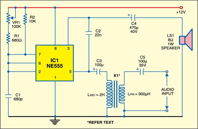
Ne 555 Amplifier Circuit Diagram. Low power audio amplifier using 555 timer. Circuits into the ever increasing ranks of timer users.
The ic can operate in three different modes such as astable monotstable and bistable because of which it can be adapted into many types of circuit designs like time delay circuits pulse generation circuit oscillator circuit and much more. Control pin 5 is the point of 2 3vcc inside the 555 timer ic so we can change this 2 3vcc voltage through this pin. Ne555 se555c sa555 16 v pd maximum allowable power dissipation 1 600 mw ta operating ambient temperature range ne555 0 to 70 c sa555 40 to 85 c se555 se555c 55 to 125 c tstg storage temperature range 65 to 150 c tsold lead soldering temperature 10sec max 300 c notes.
Control pin 5 is the point of 2 3vcc inside the 555 timer ic so we can change this 2 3vcc voltage through this pin.
Ne555 is a very popular ic among electronics hobbyists and students. Circuit diagram of a low power audio amplifier using 555 timer electronics hub circuit design of low power audio amplifier. Datasheet pinout circuit diagram inside. Learn how does ne555 timer work.
